EnSilica opens engineering hub on Cambridge Science Park
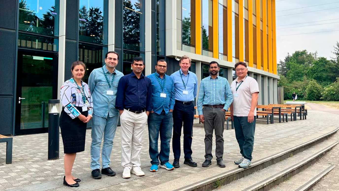
Drawing on Cambridge's renowned semiconductor ecosystem, EnSilica has opened a new engineering facility in the city and recruited six engineers, four of whom hold PhDs, increasing the company's global workforce to 190.
With the addition of this new facility and technical expertise, EnSilica will expand its existing mmWave / RF integrated circuit design capabilities – an area in which the company has already seen significant customer demand.
The expansion has been facilitated by a recent UK Space Agency C-LEO funded award, alongside additional contract momentum and customer wins that continue to support the company's growth.
EnSilica currently operates across three UK engineering design centres in Abingdon, Sheffield and Bristol, alongside additional international engineering facilities in Bangalore, India, and Porto Alegre and Campinas in Brazil.
Ian Lankshear, CEO of EnSilica, said: "We are delighted to have not only secured a team of highly skilled engineers at a time when there is a very real shortage of engineering talent in the UK, but also to establish a firm base in an established UK tech hub like Cambridge which ideally positions the business to attract additional talent.
“By further expanding our engineering knowhow across the satellite and communications market, I believe that this investment will enable the business to capitalise further on very real and near-term growth opportunities."
The arrival in Cambridge makes a lot of sense: EnSilica is a key member of the Arm Approved design partner programme which is a global network of design service companies endorsed by the Cambridge headquartered superchip architect.